-
temp Imprint CVD Inorganic Strontium domain_switching KPFM thermoplastic_elastomers Nickel HighResolution HBN LowDensityPolyethylene organic_polymer alkanes C60H122 LiquidImaging SThM polyvinyl acetate AdhesionForce layers Hydroxyapatite UnivCollegeLondon hard_disk ForceMapping FuelCell PDMS Lift Optical Yeditepe_University Regensburg LMF SelfAssembly Sulfur Floppy TriGlycineSulphate
Report image
If you found this image unacceptable, please let us know. We will review your report and take action if we determine this image is really unacceptable.
Semiconductor device, Failure analysis
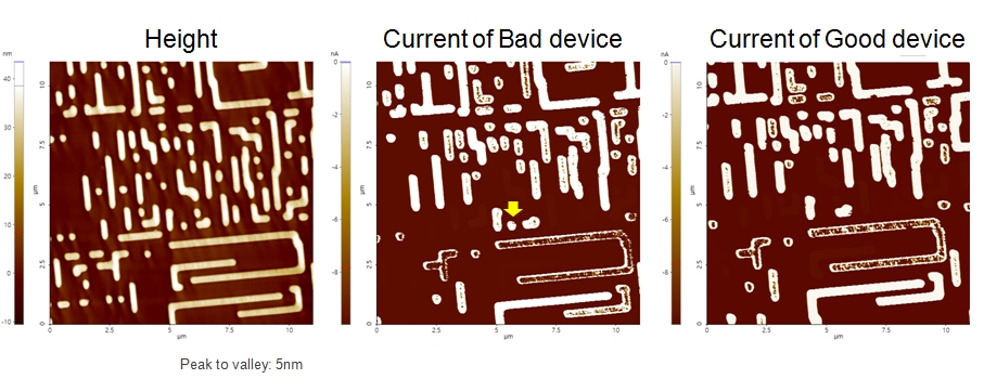
Scanning Conditions
- System: NX10
- Scan Mode: Conductive AFM
- Cantilever: CDT-Contr (k=0.5N/m, f=20kHz)
- Scan Size: 11μm×11μm
- Scan Rate: 1Hz
- Pixel: 512×512
- Sample bias: -0.5V