-
PMNPT Chrome IcelandSpar LiquidImaging kelvin probe force microscopy hard_disk_media ChemicalCompound FAFailureAnlaysis InsulatorFilm CP-AFM AIN Chemical_Vapor_Deposition HighResolution Ceramic ForceVolumeMapping Vortex fluoroalkane Polyaniline FastScan Bismuth Reduction molecule Writing self-assembly Lateral_Force_Microscopy Current Conductance Hafnia HafniumDioxide SFAs IndiumTinOxide CrAu Sic CntFilm Patterns
Report image
If you found this image unacceptable, please let us know. We will review your report and take action if we determine this image is really unacceptable.
Semiconductor device, W-plug
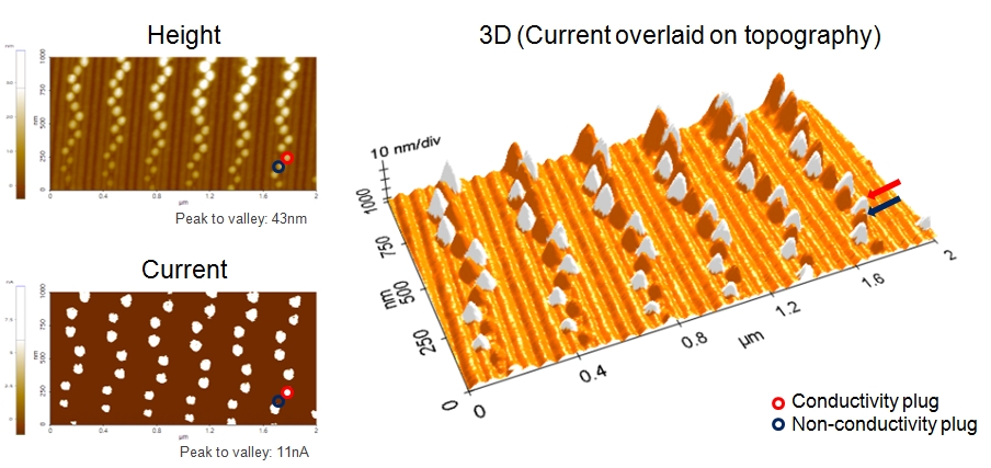
Scanning Conditions
- System: NX10
- Scan Mode: Conductive AFM
- Cantilever: ElectriMulti75-G (k=3N/m, f=75kHz)
- Scan Size: 2μm×1μm
- Scan Rate: 0.3Hz
- Pixel: 512×256
- Sample bias: +1V