-
GaAs Hole temperature controller AFM silicon_carbide MoS2 Piezoresponse Phosphide Stiffness Nanostructure ULCA Galfenol Ferroelectric PMNPT ForceVolumeImage graphene_hybrid Polarization Tapping OpticalWaveguide Polyurethane Tungsten hydrocarbon IVSpectroscopy SetpointMode cannabinoid Corrosion AdhesionEnergy exfoliate thermal_property Pinpoint PFM HardDisk Ni81Fe19 temperature_control Sidewall TungstenDeposition STM
Report image
If you found this image unacceptable, please let us know. We will review your report and take action if we determine this image is really unacceptable.
Monolayer Graphene on PDMS Surface
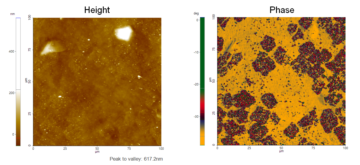
Monolayer Graphene grown on Cu foil using CVD process is transferred on to PDMS substrate.
Scanning Conditions
- System: NX20
- Scan Mode: Tapping
- Cantilever: Access-NC (k=113N/m, f=330kHz)
- Scan Size: 100μm×100μm
- Scan Rate: 0.6Hz
- Pixel Size: 256 × 256
- Scan Mode: Tapping
- Cantilever: Access-NC (k=113N/m, f=330kHz)
- Scan Size: 100μm×100μm
- Scan Rate: 0.6Hz
- Pixel Size: 256 × 256