-
membrane PVAC Lattice Thermal Polyaniline ring shape Heat IIT-chennai temp HardDisk ElectroDeposition electrospinning CompactDisk Polyvinylidene TiO2 pulsed_laser_deposition Optic GlassTemperature Thermoplastic_polyurethane Hafnium_dioxide MonoLayer ContactMode LateralForceMicroscopy Ananth Conduct biocompatible Temasek_Lab Yttria_stabilized_Zirconia Austenite ReflexLens Potential TungstenThinFilmDeposition mechanical property PVA PhaseTransition
Report image
If you found this image unacceptable, please let us know. We will review your report and take action if we determine this image is really unacceptable.
Taegeuk Mark Lithography on PZT
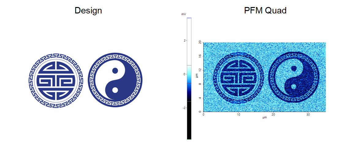
Re-arranged the domain pole direction on PZT surface using bias mode of lithography.
Scanning Conditions
- System: NX10
- Scan Mode: Lithography
- Cantilever: PPP-ContScPt (k=0.2N/m, f=25kHz)
- Scan Size: 35μm×20μm
- Scan Rate: 0.5Hz
- Pixel Size: 1024 × 1024
- Tip Bias: 10V for patterned area
- Scan Mode: Lithography
- Cantilever: PPP-ContScPt (k=0.2N/m, f=25kHz)
- Scan Size: 35μm×20μm
- Scan Rate: 0.5Hz
- Pixel Size: 1024 × 1024
- Tip Bias: 10V for patterned area