-
Oxide Hair Optic IcelandSpar Aluminium_Oxide Monisha LithiumNiobate PhaseTransition LateralForce hydrocarbon Chemical Vapor Deposition Edwin Reading ReflexLens Perovskite PUR Optoelectonics Device RedBloodCell Stiffness 3-hexylthiophene Forevision phase_change TransitionMetal MoS2 LeakageCurrent nanomechanical C60H122 cannabidiol Battery Adhesive Heating ThermalProperties HfO2 Molybdenum_disulfide
Report image
If you found this image unacceptable, please let us know. We will review your report and take action if we determine this image is really unacceptable.
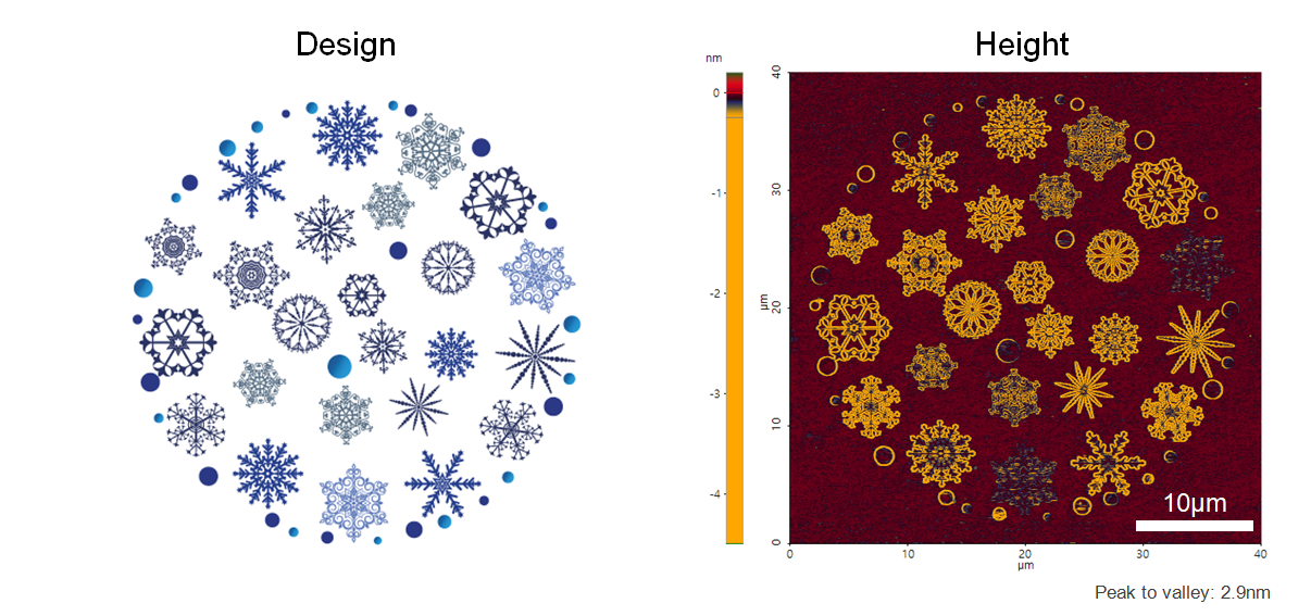
Christmas Ball Lithography on Si

Create oxidation layers on bare Si surface using bias mode of lithography.
Scanning Conditions
- System: NX10
- Scan Mode: Lithography
- Cantilever: AD-40-SS (k=40N/m, f=200kHz)
- Scan Size: 40μm×40μm
- Scan Rate: 0.5Hz
- Pixel Size: 1024 × 1024
- Tip Bias: -10V for patterened area
- Scan Mode: Lithography
- Cantilever: AD-40-SS (k=40N/m, f=200kHz)
- Scan Size: 40μm×40μm
- Scan Rate: 0.5Hz
- Pixel Size: 1024 × 1024
- Tip Bias: -10V for patterened area
