-
PolymerBlend Conductance Ceramics Ucl FM_SKPM Bismuth Barium_titanate Holes NtuEee AlkaneFilm Cell IcelandSpar Graphite SelfAssembly Vortex Mechanical&nanotechnology MfmPhase Subhajjit FrictionalForceMicroscopy Christmas PtfeMembrane ItoGlass Ferrite semifluorinated_alkane MESA structure PolyvinylAcetate Graphene Sidewall I-VSpectroscopy epitaxy PVAP3HT Reduction MolybdenumDisulfide Conduct Phosphide
Report image
If you found this image unacceptable, please let us know. We will review your report and take action if we determine this image is really unacceptable.
Magnetic device
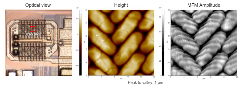
Scanning Conditions
- System : NX20
- Lift Height : 50nm
- Scan Mode: MFM
- Scan Rate : 0.3Hz
- Scan Size : 20μm×20μm
- Pixel Size : 512×256
- Cantilever : PPP-MFMR (k=2.8N/m, f=75kHz)