-
RedBloodCell SicMosfet Water Hexylthiophene HDD INSP electrospinning dichalcogenide frequency_modulation Hysteresys VinylAlcohol Mapping Polydimethylsiloxane LiftMode Praseodymium molecule FailureAnlaysis NUS Subhajjit Ni-FeAlloy CancerCell SiliconeOxide Memory ThermalDetectors Patterns FAFailureAnlaysis Writing Collagen #Materials Vortex Cross-section MultiLayerCeramicCapacitor Pinpoint PFM MonoLayer Yeditepe_University
Report image
If you found this image unacceptable, please let us know. We will review your report and take action if we determine this image is really unacceptable.
Multi-layer necking device defect
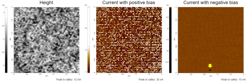
Scanning Conditions
- System : NX-Wafer
- Scan Mode: C-AFM
- Scan Rate : 2Hz
- Scan Size : 2μm×2μm
- Pixel Size : 512×256
- Cantilever : AD-2.8-AS (k=2.8N/m, f=75kHz)