-
Mechinical Boron Worcester_Polytechnic_Institute norganic CrystalGrowing CalciumHydroxide NUSNNI Mfm Heating Flake BreastCancerCell PinpointPFM Growing DeflectionOptics SicMosfet Pores Oxide Polymer IMT_Bucharest Polydimethylsiloxane HexacontaneFilm silicon_carbide MLCC Cell ScanningSpreadingResistanceMicroscopy Nanopattern Chrome AM_KPFM Ecoli PetruPoni_Institute CancerCell AtomicLayer molecules Phthalocyanine single_layer
Report image
If you found this image unacceptable, please let us know. We will review your report and take action if we determine this image is really unacceptable.
WLI image of wafer ID mark
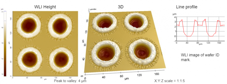
Scanning Conditions
- System : NX-Hybrid WLI
- Scan Mode: WLI
- Field of view: 182μm×182μm