-
DiffractiveOpticalElements silicon_oxide polyvinyl acetate IISCBangalore kelvin probe force microscopy Sadowski ForceVolume graphene_hybrid BismuthFerrite SelfAssembly Polyaniline Forevision ItoGlass TungstenThinFilmDeposition food blended polymers Iron Adhesion Morphology Dopped OpticalWaveguides PVAC LowDensityPolyethylene LiftHeight SKKU OpticalModulator AM_SKPM strontiu_titanate Tungsten_disulfide LiquidCrystal cross section SicMosfet LMF Magnetic Force Microscopy plastic
Report image
If you found this image unacceptable, please let us know. We will review your report and take action if we determine this image is really unacceptable.
Monolayer Graphene on PDMS Surface
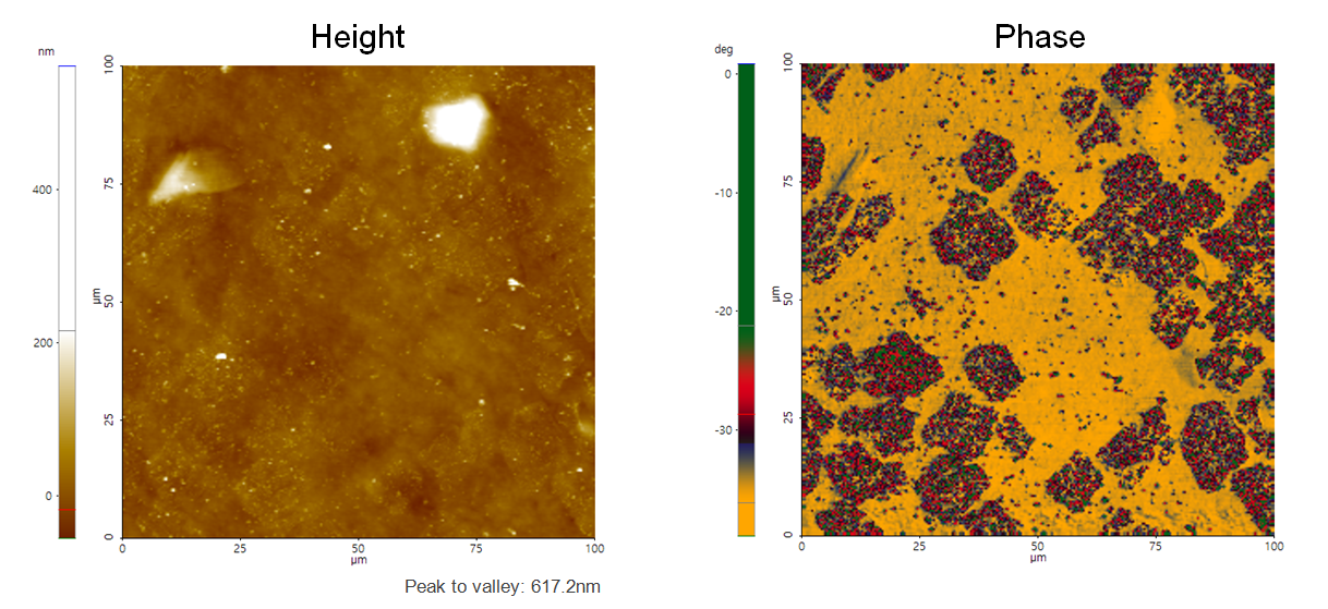
Monolayer Graphene grown on Cu foil using CVD process is transferred on to PDMS substrate.
Scanning Conditions
- System: NX20
- Scan Mode: Tapping
- Cantilever: Access-NC (k=113N/m, f=330kHz)
- Scan Size: 100μm×100μm
- Scan Rate: 0.6Hz
- Pixel Size: 256 × 256
- Scan Mode: Tapping
- Cantilever: Access-NC (k=113N/m, f=330kHz)
- Scan Size: 100μm×100μm
- Scan Rate: 0.6Hz
- Pixel Size: 256 × 256