-
Hair Force-distance Tin disulfide solar_cell MESA structure Patterns Croatia Self-assembledMonolayer IcelandSpar PolyimideFilm domain_switching semifluorinated_alkanes Granada Laser epitaxy Bio Polarization Sadowski Plug Microchannel FailureAnlaysis CuParticle IMT_Bucharest fluorocarbon Gallium Pipette Metal-organicComplex 2dMaterials Temasek_Lab HanyangUniv P3HT oxide_layer PhaseChange LateralForce Potential
Report image
If you found this image unacceptable, please let us know. We will review your report and take action if we determine this image is really unacceptable.
Fe Thin Films
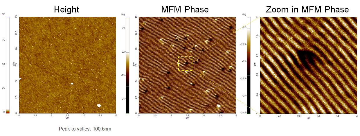
MFM images of Fe thin films (80 nm) epitaxied on GaAs(001) and then implanted with N-atoms. Images reveal weak stripe domains at magnetic remanence.
Scanning Conditions
- System: NX10
- Scan Mode: MFM
- Cantilever: PPP-MFMR (k=2.8N/m, f=75kHz)
- Scan Size: 15μm×15μm,2μm×2μm
- Scan Rate: 0.5Hz, 1Hz
- Pixel Size: 512×512, 256×256
- Lift height: 50nm
- Scan Mode: MFM
- Cantilever: PPP-MFMR (k=2.8N/m, f=75kHz)
- Scan Size: 15μm×15μm,2μm×2μm
- Scan Rate: 0.5Hz, 1Hz
- Pixel Size: 512×512, 256×256
- Lift height: 50nm