-
food Vortex Galfenol AM-KPFM self_assembly TiO2 Yttria_stabilized_Zirconia STO KAIST Chemical_Vapor_Deposition TransitionMetal exfoliate silicon_oxide Workfunction Vanadate Indent AIN small_scan Fujian OrganicSemiconductor ReflexLens LithiumNiobate Grain CBD Molybdenum lithography FrictionalForceMicroscopy Morphology Permalloy blended polymers Electical&Electronics Sio2 EPFL TemperatureControllerAFM SSRM
Report image
If you found this image unacceptable, please let us know. We will review your report and take action if we determine this image is really unacceptable.
Nanopatterened Graphene on Boron Nitride
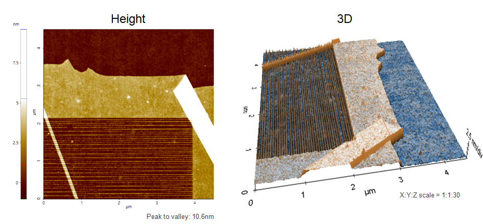
Scanning Conditions
- System: NX10
- Scan Mode: Non-contact
- Cantilever: AC160TS (k=26N/m, f=300kHz)
- Scan Size: 4.5μm×4.5μm
- Scan Rate: 0.75Hz
- Pixel Size: 512×512
- Scan Mode: Non-contact
- Cantilever: AC160TS (k=26N/m, f=300kHz)
- Scan Size: 4.5μm×4.5μm
- Scan Rate: 0.75Hz
- Pixel Size: 512×512