-
Optoelectronic alkanes Inorganic_Compound Dimethicone tip_bias_mode Perovskite TyphimuriumBiofilm FAPbI3 Cobalt CVD Anneal DeflectionOptics MembraneFilter CalciumHydroxide VortexCore IMT_Bucharest ScanningIon-ConductanceMicroscopy Treatment ScanningTunnelingMicroscopy PS_PVAC Praseodymium SrO Scanning_Thermal_Microscopy Resistance HACrystal Friction Metal-organicComplex Terrace VerticalPFM HighAspect ItoGlass HDD YttriaStabilizedZirconia C36H74 YszSubstrate
Report image
If you found this image unacceptable, please let us know. We will review your report and take action if we determine this image is really unacceptable.
BN thin film on Si
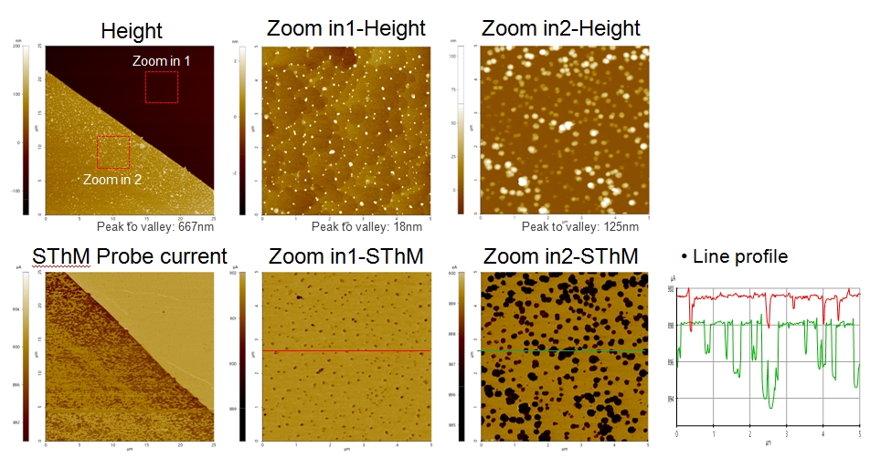
Scanning Conditions
- System: NX10
- Scan Mode:SThM
- Cantilever: Nanothermal probe
- Scan Size: 25μm×25μm, 5μm×5μm
- Scan Rate:0.3Hz, 0.5Hz
- Pixel: 256×256, 256×256
- Scan Mode:SThM
- Cantilever: Nanothermal probe
- Scan Size: 25μm×25μm, 5μm×5μm
- Scan Rate:0.3Hz, 0.5Hz
- Pixel: 256×256, 256×256