-
PDMS Biofilm conductive Magnetic SingleLayer Hexatriacontane Steps Semiconductor PiezoelectricForceMicroscopy ScanningThermalMicroscopy SmallScan OrganicSemiconductor Step NCM Anneal TyphimuriumBiofilm Growing plastic TemperatureControlledAFM CntFilm AtomicSteps Friction polyvinyl acetate AIN IISCBangalore MolybdenumDisulfide PrCurve Laser Magnetic Force Microscopy temp_control PolymerPatterns Filter Oxide Ni81Fe19 PolymerBlend
Report image
If you found this image unacceptable, please let us know. We will review your report and take action if we determine this image is really unacceptable.
MoS2 Layers on SiO2
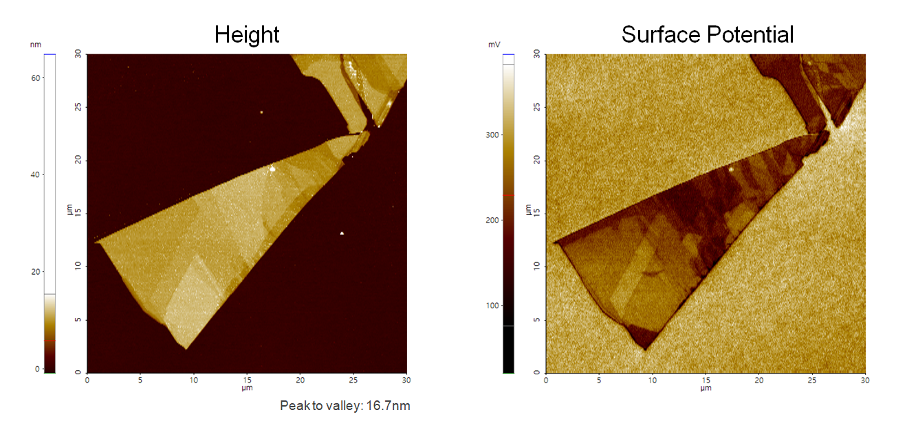
A few layers of MoS2 on SiO2
Scanning Conditions
- System: NX10
- Scan Mode: AM-KPFM
- Cantilever: NSC36Cr-Au B (k=2N/m, f=130kHz)
- Scan Size: 30μm×30μm
- Scan Rate: 0.3Hz
- Pixel Size: 512 × 256
- Scan Mode: AM-KPFM
- Cantilever: NSC36Cr-Au B (k=2N/m, f=130kHz)
- Scan Size: 30μm×30μm
- Scan Rate: 0.3Hz
- Pixel Size: 512 × 256