-
Pvdf temperature_control dielectric trench Sadowski CntFilm ConductingPolymer ShenYang mechanical property exfoliate Hair Chemical Vapor Deposition Annealed CuParticle Zagreb NanoLithography NUS_NNI_Nanocore Terrace Corrosion BismuthVanadate SKPM LateralPFM TemperatureControlledAFM organic_polymer Protein AlkaneFilm Topography ferromagnetic MBE Gallium Multiferroic_materials IVSpectroscopy LiquidCrystal 2d_materials FM_KPFM CuSubstrate
Report image
If you found this image unacceptable, please let us know. We will review your report and take action if we determine this image is really unacceptable.
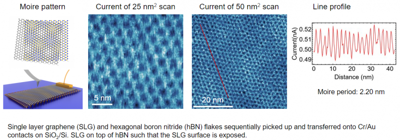
Graphene on hBN
Scanning Conditions
- System : FX40
- Sample bias: 1 V
- Scan Mode: C-AFM
- Scan Rate : 25 Hz for 25 nm2, 10 Hz for 50 nm2
- Scan Size : 25nm2×25nm2
- Pixel Size : 128×128 for 25 nm2, 256×256 for nm2
- Cantilever : ElectricMulti75-G (k=3N/m, f=75kHz)