-
Sadowski Graphite VortexCore Beads Pvdf GaN PolyvinylideneFluoride dielectric_trench VerticalPFM Annealed NUS_Physics doped Aluminum Silver SiliconOxide thermoplastic_elastomers Vanadate MonoLayer PyroelectricDetector PhaseChange Steps Sapphire Memory Galfenol Kevlar Leakage Polyethylene UnivCollegeLondon TungstenThinFilmDeposition C36H74 PECurve single_layer MechanicalProperties fe_nd_b dielectric trench
Report image
If you found this image unacceptable, please let us know. We will review your report and take action if we determine this image is really unacceptable.
Multi-layer necking device defect
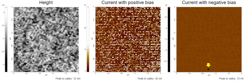
Scanning Conditions
- System : NX-Wafer
- Scan Mode: C-AFM
- Scan Rate : 2Hz
- Scan Size : 2μm×2μm
- Pixel Size : 512×256
- Cantilever : AD-2.8-AS (k=2.8N/m, f=75kHz)