-
Biofilm VerticalPFM BismuthVanadate Graphite align YttriaStabilizedZirconia Edwin CuParticle Liquid PetruPoni Global_Comm fluoroalkane nanomechanical Conductive AFM UTEM Wildtype BCZT MultiLayerCeramicCapacitor Resistance FrictionalForce Dental NanoLithography Materials Oxidation Worcester_Polytechnic_Institute ScanningTunnelingMicroscopy Barium_titanate Force-distance AM-KPFM PolyvinylideneFluoride Subhajjit LiftHeight Optoelectronic Sapphire cannabis
Report image
If you found this image unacceptable, please let us know. We will review your report and take action if we determine this image is really unacceptable.
MoS2 Layers on SiO2
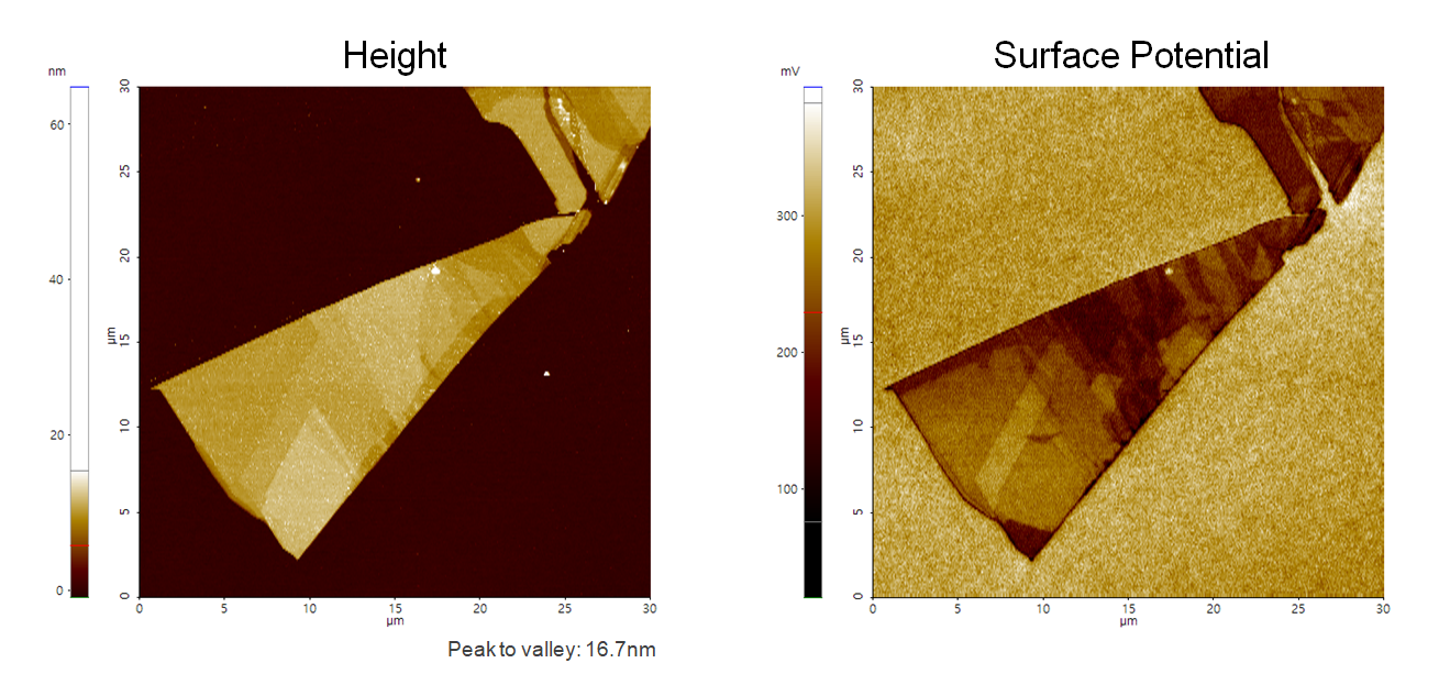
A few layers of MoS2 on SiO2
Scanning Conditions
- System: NX10
- Scan Mode: AM-KPFM
- Cantilever: NSC36Cr-Au B (k=2N/m, f=130kHz)
- Scan Size: 30μm×30μm
- Scan Rate: 0.3Hz
- Pixel Size: 512 × 256
- Scan Mode: AM-KPFM
- Cantilever: NSC36Cr-Au B (k=2N/m, f=130kHz)
- Scan Size: 30μm×30μm
- Scan Rate: 0.3Hz
- Pixel Size: 512 × 256