-
Modulus temp NiFe ReflexLens SRAM I-VSpectroscopy Collagen Sidewall LiquidCrystal PetruPoni Heat NUSNNI FM_KPFM cooling TemperatureControl CrossSection Multiferroic_materials AdhesionForce IndiumTinOxide Electrode MechanicalProperties Inorganic_Compound self-assembled_monolayer UnivOfMaryland HexacontaneFilm Nanopattern CBD CalciumHydroxyapatite PANI Layer Force-distance P3HT Tin sulfide LaAlO3 IIT-chennai
Report image
If you found this image unacceptable, please let us know. We will review your report and take action if we determine this image is really unacceptable.
Trench Etch Profile on MESA
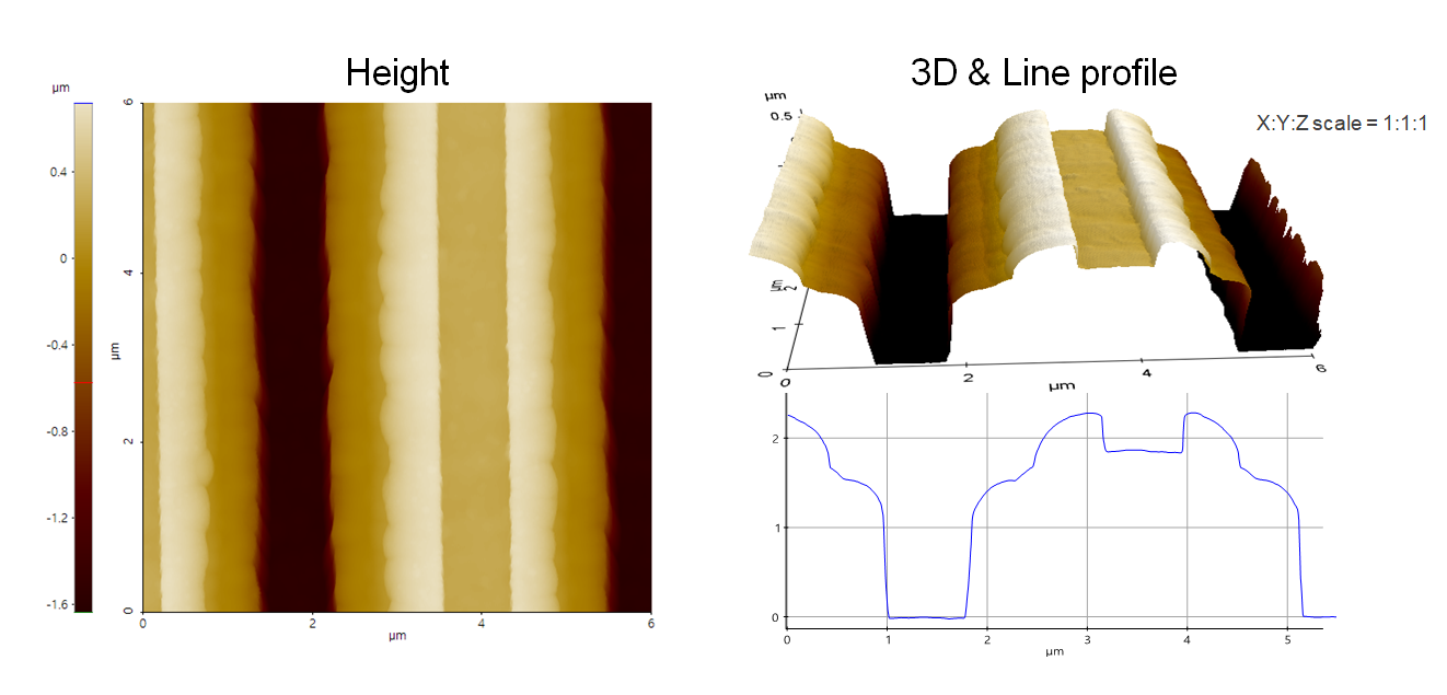
Top dielectric trench etch profile on MESA on Si wafer.
Scanning Conditions
- System: NX20
- Scan Mode: Non-contact
- Cantilever: AR5T-NCHR (k=42N/m, f=300kHz)
- Scan Size: 6μm×6μm
- Scan Rate: 0.12Hz
- Pixel Size: 1024 × 256
- Scan Mode: Non-contact
- Cantilever: AR5T-NCHR (k=42N/m, f=300kHz)
- Scan Size: 6μm×6μm
- Scan Rate: 0.12Hz
- Pixel Size: 1024 × 256