-
CuSubstrate ScanningThermalMicroscopy Layer GaAs BreastCancerCell Liquid SmallScan Conducting Wafer Phase small_scan Magnetic Force Microscopy BoronNitride IIT-chennai SingleLayer StainlessSteel Non-ContactMode Inorganic_Compound ChemicalCompound mechanical property Nanopattern C60H122 FM-KPFM CalciumHydroxide Aggregated_molecules China ConductiveAFM C36H74 Polarization electrospinning NiFe Pzt PS_LDPE LowDensityPolyethylene Oxide
Report image
If you found this image unacceptable, please let us know. We will review your report and take action if we determine this image is really unacceptable.
Atomic steps on GaP(Gallium Phosphide) layer on Si
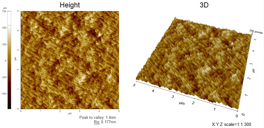
Scanning Conditions
- System: NX20
- Scan Mode: Non-contact
- Cantilever: PPP-NCHR (k=42N/m, f=300kHz)
- Scan Size: 5μm×5μm
- Scan Rate: 1Hz
- Pixel: 512×512