-
HexagonalBN Magnetostrictive Christmas Pinpoint PFM VortexCore Ucl plastic Insulator FrictionForce Annealed temp_control Dimethicone Change Domain IISCBangalore Conductive AFM temperature controller AFM Chungnam_National_University FM_KPFM Thermoplastic_polyurethane STM Friction PECurve SiliconOxide Fujian Aluminium_Oxide Hair Fluoride LateralPFM ForceVolumeImage Grain NCM\ Roughness Strontium Optical
Report image
If you found this image unacceptable, please let us know. We will review your report and take action if we determine this image is really unacceptable.
SiC MOSFET
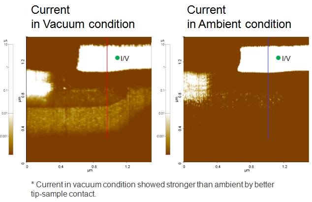
Scanning Conditions
- System: NX-Hivac
- Scan Mode: SSRM
- Cantilever: Full diamond (k=27 N/m)
- Scan Size: 2μm×2μm
- Scan Rate: 0.5Hz
- Pixel: 256×512
- Sample Bias: +2.5V
- Scan Mode: SSRM
- Cantilever: Full diamond (k=27 N/m)
- Scan Size: 2μm×2μm
- Scan Rate: 0.5Hz
- Pixel: 256×512
- Sample Bias: +2.5V