-
ElectrostaticForceMicroscopy MESA structure AdhesionForce CarbonNanotube LithiumNiobate PinpointNanomechanicalMode Temasek_Lab LifeScience GlassTemp Scratch Phase Pipette PtfeFilter TPU PhaseChange Annealing FrictionForce Filter PvdfBead SurfaceOxidation OpticalModulator LightEmiting neodymium_magnets Hydroxyapatite LiNbO3 ScanningKelvinProbeMicroscopy ito_film Tin sulfide ContactMode C_AFM fluoroaalkane Iron SrO Ucl Formamidinium_lead_iodide
Report image
If you found this image unacceptable, please let us know. We will review your report and take action if we determine this image is really unacceptable.
Photoresist pattern (post-development process)
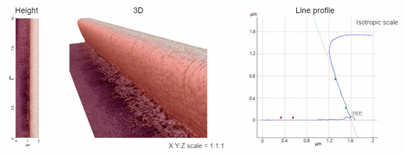
Scanning Conditions
- System : NX-3DM
- Scan Mode: Non-contact
- Scan Rate : 0.1 Hz
- Scan Size : 2μm×10μm
- Pixel Size : 512×2048
- Cantilever : EBD-R2-NCLR (k=45N/m, f=190kHz)