-
Ecoli UnivCollegeLondon TriGlycineSulphate INSP C_AFM plastic OrganicSemiconductor Pattern PMNPT Hysteresys BiFeO3 Temperature OpticalModulator rubber ScanningThermalMicroscopy Pores Photovoltaics Fiber AdhesionForce atomic_steps Polymer MfmAmplitude Floppy FFM MLCC InLiquid SmalScan #EC Pzt SurfaceOxidation conductive CuSubstrate Polarization Graphene Pipette
Report image
If you found this image unacceptable, please let us know. We will review your report and take action if we determine this image is really unacceptable.
MoS2 Layers on SiO2
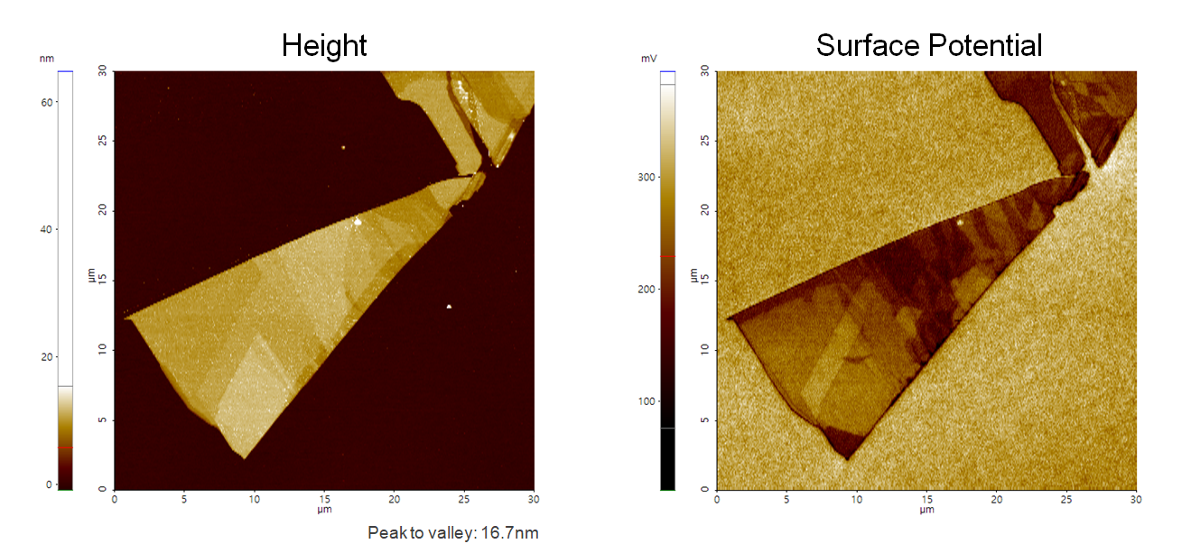
A few layers of MoS2 on SiO2
Scanning Conditions
- System: NX10
- Scan Mode: AM-KPFM
- Cantilever: NSC36Cr-Au B (k=2N/m, f=130kHz)
- Scan Size: 30μm×30μm
- Scan Rate: 0.3Hz
- Pixel Size: 512 × 256
- Scan Mode: AM-KPFM
- Cantilever: NSC36Cr-Au B (k=2N/m, f=130kHz)
- Scan Size: 30μm×30μm
- Scan Rate: 0.3Hz
- Pixel Size: 512 × 256