-
flakes solar_cell cross section HighResolution Reading Polystyrene heterojunctions Copolymer DiffractiveOpticalElements Thermoplastic_polyurethane NanoLithography SelfAssembly LogAmplifier Ceramics Ananth TriGlycineSulphate PVAP3HT Forevision WPlug VerticalPFM TungstenThinFilmDeposition Inorganic_Compound CrossSection SetpointMode H-BN Logo CuSubstrate PyroelectricDetector C60H122 SingleLayer HydroGel Phase ImideMonomer AAO Gallium_Arsenide
Report image
If you found this image unacceptable, please let us know. We will review your report and take action if we determine this image is really unacceptable.
Trench Etch Profile on Si Wafer
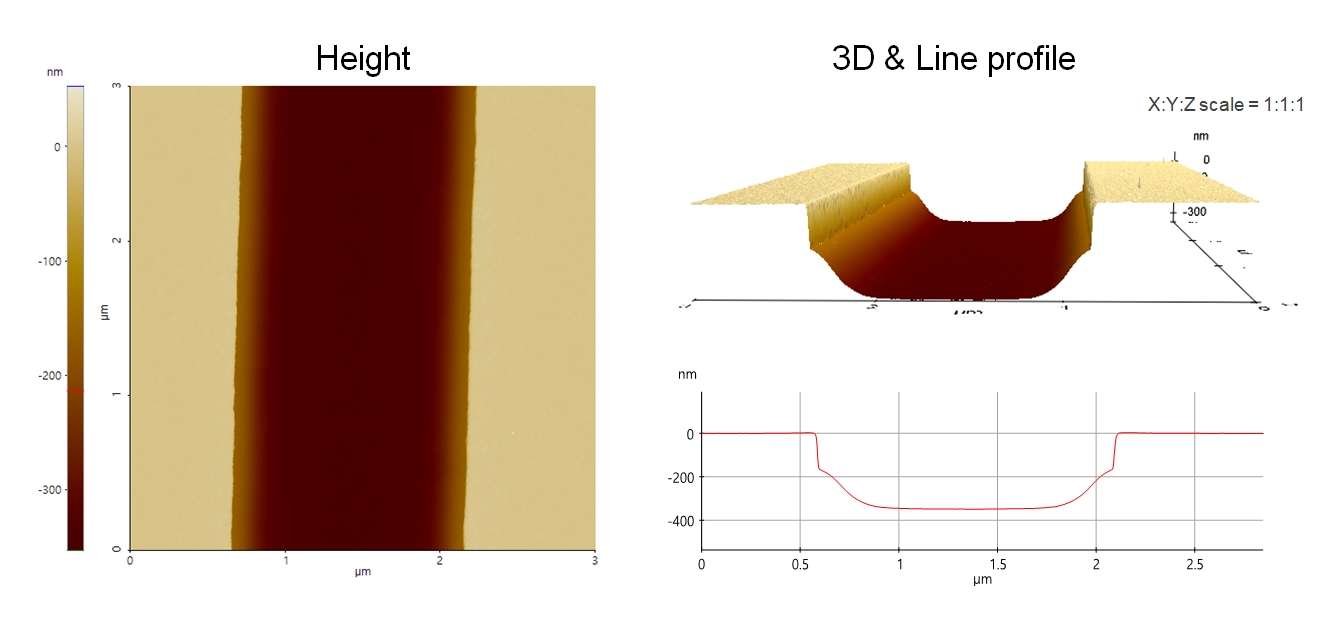
Top dielectric trench etch profile on Si wafer having tapered slope at the trench sidewall.
Scanning Conditions
- System: NX20
- Scan Mode: Non-contact
- Cantilever: AC160TS (k=26N/m, f=300kHz)
- Scan Size: 3μm×3μm
- Scan Rate: 0.21Hz
- Pixel: 1024 × 256
- Scan Mode: Non-contact
- Cantilever: AC160TS (k=26N/m, f=300kHz)
- Scan Size: 3μm×3μm
- Scan Rate: 0.21Hz
- Pixel: 1024 × 256