-
MechanicalProperties rubber 2dMaterials ElectroChemical Imprint BFO SPMLabs LiquidCrystal Flake MoS2 Crystal Ni-FeAlloy PolymerBlend LaAlO3 KAIST IndiumTinOxide AM_SKPM DeoxyribonucleicAcid HighAcpectRatio Composition CntFilm FailureAnalysis Thermoplastic_polyurethane Hexylthiophene Polyimide cannabis ConductiveAFM SKPM DentalProsthesis exfoliate Cell Praseodymium Etch MBE LogAmplifier
Report image
If you found this image unacceptable, please let us know. We will review your report and take action if we determine this image is really unacceptable.
Trench Etch Profile on MESA
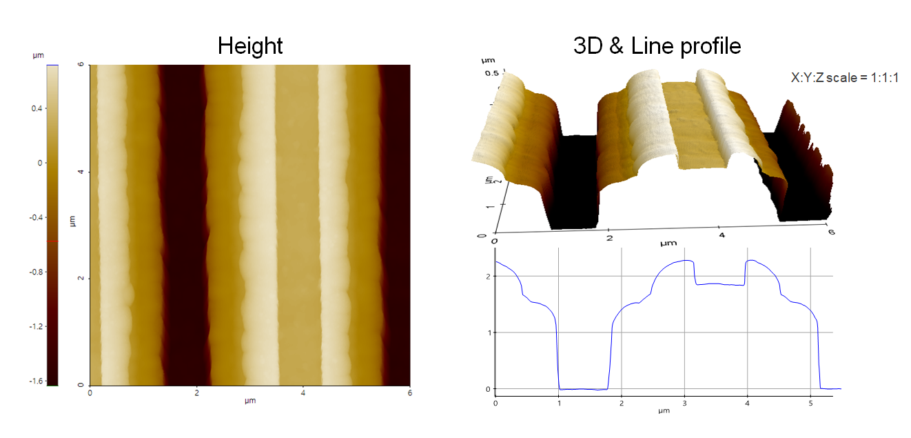
Top dielectric trench etch profile on MESA on Si wafer.
Scanning Conditions
- System: NX20
- Scan Mode: Non-contact
- Cantilever: AR5T-NCHR (k=42N/m, f=300kHz)
- Scan Size: 6μm×6μm
- Scan Rate: 0.12Hz
- Pixel Size: 1024 × 256
- Scan Mode: Non-contact
- Cantilever: AR5T-NCHR (k=42N/m, f=300kHz)
- Scan Size: 6μm×6μm
- Scan Rate: 0.12Hz
- Pixel Size: 1024 × 256