-
#EC WWafer Polyaniline LiNbO3 CaMnO3 PolyvinylAcetate HardDisk Wonseok LifeScience WPlug Composition Photovoltaics Graphite UnivOfMaryland IRDetector piezoelectric force microscopy Edwin Gong fluoroalkane DNAProtein NUS_NNI_Nanocore HighAspect contact Magnetic Silver AnodizedAluminumOxide FAPbI3 Neodymium Foil IndiumTinOxide Celebration FFM MechanicalProperties LMF OrganicCompound
Report image
If you found this image unacceptable, please let us know. We will review your report and take action if we determine this image is really unacceptable.
ITO Film Sputter Deposited onto Silicon
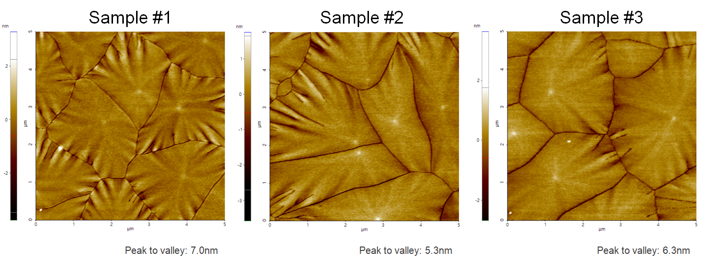
ITO-film, which was sputter deposited onto silicon. The grain size of those samples was influenced by changing the process settings in the Cluterline RAD sputter deposition system, one of the deposition tool platforms manufactured by Evatec.
Scanning Conditions
- System: NX10
- Scan Mode: Non-contact
- Cantilever: PPP-EFM (k=2.8N/m, f=75kHz)
- Scan Size: 5μm×5μm
- Scan Rate: 0.1Hz
- Pixel Size: 256 × 256
- Scan Mode: Non-contact
- Cantilever: PPP-EFM (k=2.8N/m, f=75kHz)
- Scan Size: 5μm×5μm
- Scan Rate: 0.1Hz
- Pixel Size: 256 × 256