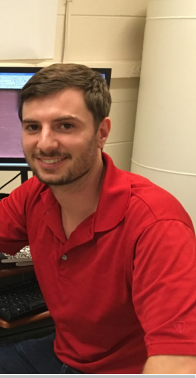
JEAN-PHILIPPE TURMAUD
JEAN-PHILIPPE TURMAUD was born near Lyon, France in 1990. Growing up on the country side and regularly escaping into the Alps, he developed a curiosity towards nature, weather phenomena and science in general. Learning more about basics physics in high school lead him to choose a higher education in engineering and physics. He graduated with a Master of science in engineering physics from Grenoble Institute of Technology and the Royal Institute of Technology in Stockholm. Now, he is working on getting his PhD in Physics from Georgia Tech where his research focuses on the electronic properties of different forms of epitaxial graphene on silicon carbide.
Park AFM Scholarship Winner , Jean-Philippe Turmaud currently working on his PhD in Physics from Georgia Tech where his research focuses on the electronic properties of different forms of epitaxial graphene on silicon carbide. He characterizes samples by Raman spectroscopy, AFM, XPS and ARPES to confirm their structural properties and produce electronic devices on single SiC terraces.
"OUR PARK AFM ALLOWS US TO ANSWER CRUCIAL QUESTIONS ABOUT THE STRUCTURE OF THE SURFACE OF OUR MATERIAL: DID WE PRODUCE A SURFACE COVERED WITH GRAPHENE? WHAT IS THE SIZE OF THE GRAPHENE RIBBONS WE ARE GOING TO INVESTIGATE? IS THERE ANY KIND OF CONTAMINATION? WHAT IS THE ROUGHNESS OF THE SURFACE?" JEAN-PHILIPPE TURMAUD
The confinement control sublimation is used to produce high quality epitaxial graphene on SiC for nanoelectronics. We report here on the experimental investigation of the first graphene layer grown on SiC(0001) (the buffer layer). The buffer layer is a semiconducting form of graphene, with a gap in the density of state previously probed by ARPES and STM measurement. We characterize our samples by Raman spectroscopy, AFM, XPS and ARPES to confirm their structural properties and produce electronic devices on single SiC terraces. The temperature and electrical field dependence of the bulk conductivity of the buffer layer are investigated and the effects of contacts and gas adsorption are considered. The observed behavior seem to be related to the known structural periodicity of the buffer layer.
How do you think your research will impact society in a positive way?
There is no doubt that today's society is profoundly shaped by our use of technology. From renewable energy production to self driving cars, the need for cheap but efficient functional materials is constantly increasing. The development of the silicon industry was only possible through years of research on the fundamental and practical properties of semiconductors. In the same way, materials of future application need the same fundamental knowledge of their properties. My research is oriented towards that goal. It focuses on understanding the electronic transport in epitaxial graphene, a promising candidate as a successor to silicon in many applications. My project aims to bring light onto limiting factors of electrical conduction in novel two dimensional materials like graphene, to eventuality overcome them and produce competitive devices.
What is the best or most useful part of using Park AFM for your research?
Prior to building devices with epitaxial graphene on silicon carbide, it is essential to know the structure of the surface of our material: did we produce a surface covered with graphene? What is the size of the graphene ribbons we are going to investigate? Is there any kind of contamination? what is the roughness of the surface? Our Park AFM allows us to answer those crucial questions. The most powerful mode we use is the Lateral Force Microscopy. It allows us, with excellent resolution to measure the local friction of the surface and discriminate between a bare silicon carbide surface, one layer of graphene and two or more layers of graphene, which all have different friction coefficients. We can then build our devices accordingly

