-
Inorganic Fe_film HighResolution ReflexLens SrTiO3 Celebration MechanicalProperties PMNPT FrictionForce LateralForce Aggregated_molecules piezoelectric force microscopy Insulator PVA ForceMapping Mosfet LiftMode Yttria_stabilized_Zirconia NCM\ Gallium_Arsenide Mapping STO LateralForceMicroscopy CancerCell NUSNNI Phase OrganicCompound light_emission strontiu_titanate Gallium FrequencyModulation ScratchMode Solar GlassTemperature Ceramic
Report image
If you found this image unacceptable, please let us know. We will review your report and take action if we determine this image is really unacceptable.
Taegeuk Mark Lithography on PZT
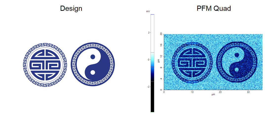
Re-arranged the domain pole direction on PZT surface using bias mode of lithography.
Scanning Conditions
- System: NX10
- Scan Mode: Lithography
- Cantilever: PPP-ContScPt (k=0.2N/m, f=25kHz)
- Scan Size: 35μm×20μm
- Scan Rate: 0.5Hz
- Pixel Size: 1024 × 1024
- Tip Bias: 10V for patterned area
- Scan Mode: Lithography
- Cantilever: PPP-ContScPt (k=0.2N/m, f=25kHz)
- Scan Size: 35μm×20μm
- Scan Rate: 0.5Hz
- Pixel Size: 1024 × 1024
- Tip Bias: 10V for patterned area