-
blended polymers SKKU Electrical&Electronics non_contact Au111 semifluorinated_alkanes TCS Polyethylene ForceDistanceSpectroscopy plastic ChemicalCompound Terrace Edwin Conducting MonoLayer Yeditepe Magnetostrictive Tape Spincast Polarization CrAu Display Fiber Celebration LaAlO3 DeoxyribonucleicAcid Platinum PinpointPFM Dimethicone molecular_beam Aluminium_Oxide Sidewall Led PolyimideFilm PolyvinylAcetate
Report image
If you found this image unacceptable, please let us know. We will review your report and take action if we determine this image is really unacceptable.
AlN/GaN/AlN Hetero Structure
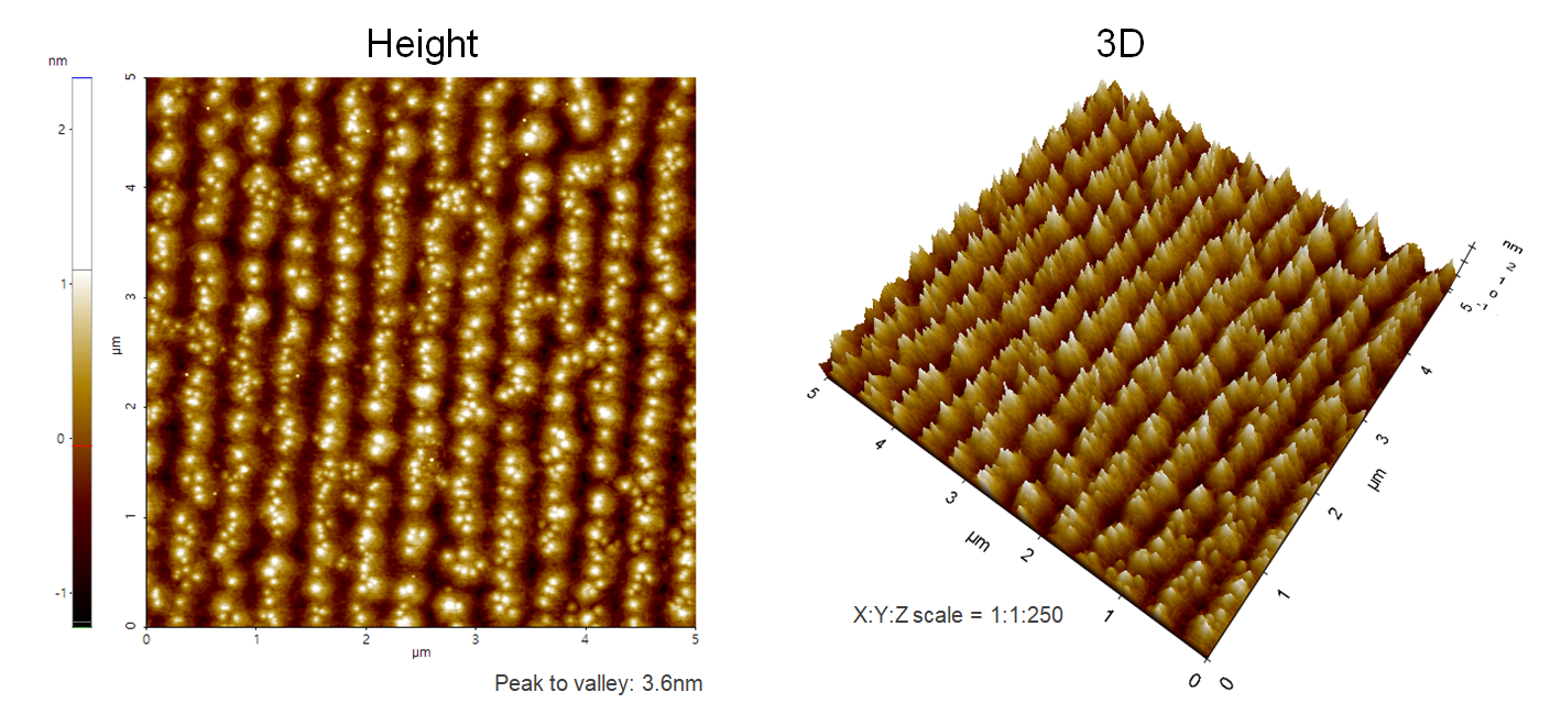
AlN/GaN/AlN hetero structure grown on SiC substrate by Molecular Beam Epitaxy (MBE) system.
Scanning Conditions
- System: NX20
- Scan Mode: Non-contact
- Cantilever: AC160TS (k=26N/m, f=300kHz)
- Scan Size: 5μm×5μm
- Scan Rate: 0.5Hz
- Pixel Size: 512 × 512
- Scan Mode: Non-contact
- Cantilever: AC160TS (k=26N/m, f=300kHz)
- Scan Size: 5μm×5μm
- Scan Rate: 0.5Hz
- Pixel Size: 512 × 512