-
FrictionalForce LiIonBattery Indent ferromagnetic Conductivity P3HT EPFL Collagen NTU 2d_materials Alloy Current suspended_graphene DiffractiveOpticalElements conductive PatternedSapphireSubstrat Boron Hexacontane NUSNNI TungstenDeposition Conductive AFM MeltingPoint self_assembly Typhimurium ScanningIon-ConductanceMicroscopy Ni-FeAlloy plastic NanoLithography Mechanical Styrene Piezoelectric norganic Polydimethylsiloxane Lattice Resistance
Report image
If you found this image unacceptable, please let us know. We will review your report and take action if we determine this image is really unacceptable.
Stitched image of chiplet
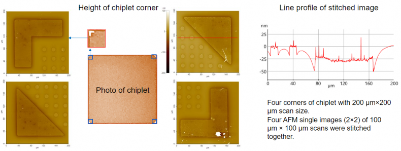
Scanning Conditions
- System : NX-Wafer
- Scan Mode: Non-contact
- Scan Rate : 0.5 Hz
- Scan Size : 100μm×100μm for single image (200μm×200μm stitched image)
- Pixel Size : 512×128 for single image
- Cantilever : OMCL-AC240TS (k=2N/m, f=70kHz)