-
Korea TemperatureControl Composite margarine PhaseChange conductive Indium_tin_oxide NUS_NNI_Nanocore IIT-chennai heterojunctions Melt SiliconOxide HOPG Permalloy fifber HydroGel Magnets Ram Resistance Alkane SAM membrane biocompatible RedBloodCell IcelandSpar Croatia Spain Magnetic Force Microscopy MagneticForceMicroscopy PatternedSapphireSubstrat Indent Strontium NCM\ Bacteria FM_KPFM
Report image
If you found this image unacceptable, please let us know. We will review your report and take action if we determine this image is really unacceptable.
GaN on Si epi film
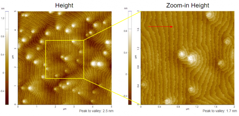
Scanning Conditions
- System : NX20
- Scan Mode: Non-contact
- Scan Rate : All 2 Hz
- Scan Size : 5µm2, 5µm2
- Pixel Size : ALL 512×512
- Cantilever : OMCL-AC160TS (k=26N/m, f=300kHz)