-
MfmPhase block_copolymer Organic WWafer ContactModeDots PpLdpe PtfeFilter SoftSample OrganicSemiconductor Graphene Adhesion LiIonBattery self-assembly Biology molecular_beam dielectric_trench ScratchMode Gallium_Arsenide Ecoli OpticalElement SRAM SThM MechanicalProperty Vanadate Dr.JurekSadowski PrCurve amplitude_modulation FFM Ananth Growth HardDiskMedia LDPE Nanotechnology ScanningSpreadingResistanceMicroscopy Electronics
Report image
If you found this image unacceptable, please let us know. We will review your report and take action if we determine this image is really unacceptable.
Taegeuk Mark Lithography on PZT
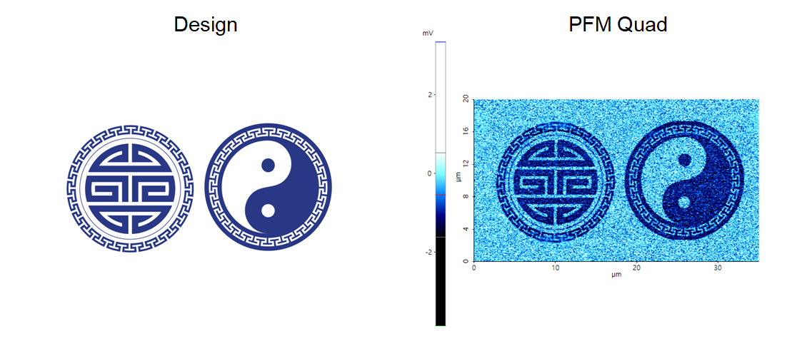
Re-arranged the domain pole direction on PZT surface using bias mode of lithography.
Scanning Conditions
- System: NX10
- Scan Mode: Lithography
- Cantilever: PPP-ContScPt (k=0.2N/m, f=25kHz)
- Scan Size: 35μm×20μm
- Scan Rate: 0.5Hz
- Pixel Size: 1024 × 1024
- Tip Bias: 10V for patterned area
- Scan Mode: Lithography
- Cantilever: PPP-ContScPt (k=0.2N/m, f=25kHz)
- Scan Size: 35μm×20μm
- Scan Rate: 0.5Hz
- Pixel Size: 1024 × 1024
- Tip Bias: 10V for patterned area