-
#EC TyphimuriumBiofilm ScanningIon-ConductanceMicroscopy Nanotechnology PDMS ito_film Multiferroic_materials DataStorage Calcium TipBiasMode Genetic thermal_conductivity DiffractiveOpticalElements Ni81Fe19 Wonseok SelfAssembly DIWafer flakes TungstenDeposition OpticalWaveguide Device molecular_self_assembly temp_control hydrocarbon PhaseImaging GaAs F14H20 HighResolution Boundary Hafnia Aggregated_molecules Tungsten_disulfide Fujian bias_mode Neodymium
Report image
If you found this image unacceptable, please let us know. We will review your report and take action if we determine this image is really unacceptable.
Trench Etch Profile on Si Wafer
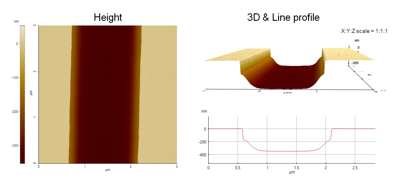
Top dielectric trench etch profile on Si wafer having tapered slope at the trench sidewall.
Scanning Conditions
- System: NX20
- Scan Mode: Non-contact
- Cantilever: AC160TS (k=26N/m, f=300kHz)
- Scan Size: 3μm×3μm
- Scan Rate: 0.21Hz
- Pixel: 1024 × 256
- Scan Mode: Non-contact
- Cantilever: AC160TS (k=26N/m, f=300kHz)
- Scan Size: 3μm×3μm
- Scan Rate: 0.21Hz
- Pixel: 1024 × 256