-
Mfm Spain Pinpoint PFM Vacuum Liquid Switching SiliconeOxide MolecularSelfAssembly UnivCollegeLondon Platinum HydroGel FAFailureAnlaysis Blood Foil HfO2 Grain OrganicSemiconductor TungstenThinFilmDeposition Strontium Battery TriGlycineSulphate Mapping BismuthVanadate Tungsten_disulfide Biology Litho Chemical Vapor Deposition GaN ForceVolumeMapping molecular_self_assembly Sio2 SRAM Titanate MetalCompound graphene_hybrid
Report image
If you found this image unacceptable, please let us know. We will review your report and take action if we determine this image is really unacceptable.
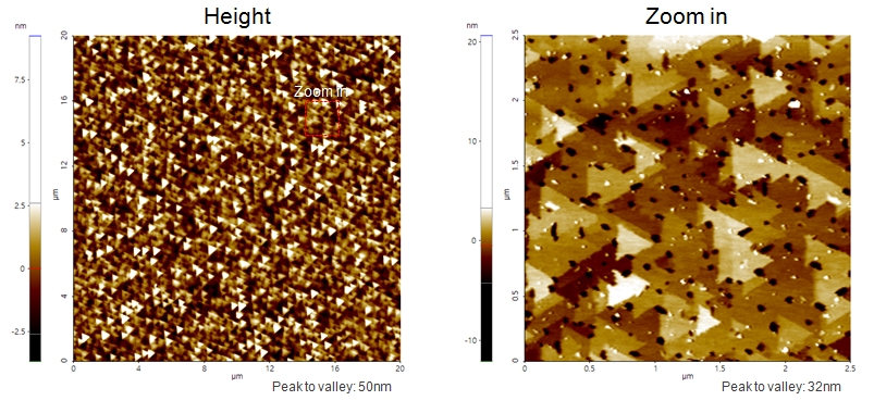
LiNbO3 wafer
Scanning Conditions
- System: NX10
- Scan Mode: Non-contact
- Cantilever: AC55TS (k=85N/m, f=1600kHz)
- Scan Size:20μm×20μm, 2.5μm×2.5μm
- Scan Rate: 5Hz, 10Hz
- Pixel: 512×512, 256×256
- Scan Mode: Non-contact
- Cantilever: AC55TS (k=85N/m, f=1600kHz)
- Scan Size:20μm×20μm, 2.5μm×2.5μm
- Scan Rate: 5Hz, 10Hz
- Pixel: 512×512, 256×256