-
ForceVolumeImage PS_PVAC InorganicCompound ScanningSpreadingResistanceMicroscopy Pores Dr.JurekSadowski CaMnO3 solar_cell Polydimethylsiloxane WWafer LightEmiting Led Polyurethane molecular_self_assembly Glass LithiumNiobate LightEmission high_resolution ReflexLens PtfeMembrane CrystalGrowing Film neodymium_magnets Yeditepe Hexatriacontane Mapping lift_mode Aggregated_molecules TPU layers CHRYSALIS_INC SrO Metal-organicComplex HexagonalBN Oxide
Report image
If you found this image unacceptable, please let us know. We will review your report and take action if we determine this image is really unacceptable.
Copper film
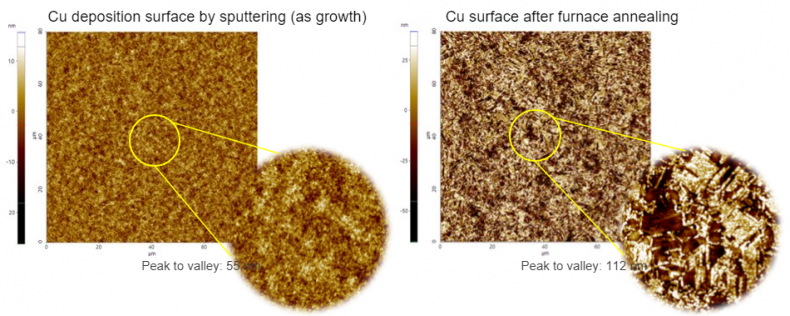
Scanning Conditions
- System : NX-Wafer
- Scan Mode: Non-contact
- Scan Rate : All 1Hz
- Scan Size : All 512μm×256μm
- Pixel Size : 512×512
- Cantilever : OMCL-AC160TS (k=26N/m, f=300kHz)