-
EvatecAG OrganicSemiconductor hard_disk high_resolution Permalloy ForceVolumeMapping TempControl GranadaUniv BTO IISCBangalore TemperatureControllerStage PolymerBlend Wildtype PVAC sputter Imprint Dimethicone temperature controller AFM Adhesion pinpoint mode TPU KPFM Indium_tin_oxide TransitionMetal Change Carbon UnivOfMaryland KAIST Scanning_Thermal_Microscopy self_assembly Piezoresponse Electrical&Electronics SrTiO3 semifluorinated alkane Ucl
Report image
If you found this image unacceptable, please let us know. We will review your report and take action if we determine this image is really unacceptable.
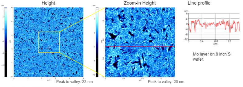
Mo film

Scanning Conditions
- System : NX-Wafer
- Scan Mode: Non-contact
- Scan Rate : 0.5 Hz, 0.8 Hz
- Scan Size : 5μm2, 15μm2
- Pixel Size : All 1024×512
- Cantilever : OMCL-AC160TS (k=26N/m, f=300kHz)
