-
TemperatureControllerStage Bio #Materials Graphene single_layer PrCurve Holes StyreneBeads Magnets Defect CP-AFM I-VSpectroscopy self-assembly AdhesionForce align chemical_compound Lattice epitaxy Led Pvdf LithiumNiobate AtomicSteps TCS Ananth ForceVolumeMapping neodymium_magnets Edwin HumanHair Chloroform Grain Stiffness layers SThM Oxidation MLCC
Report image
If you found this image unacceptable, please let us know. We will review your report and take action if we determine this image is really unacceptable.
Carbon Nanotube on Si
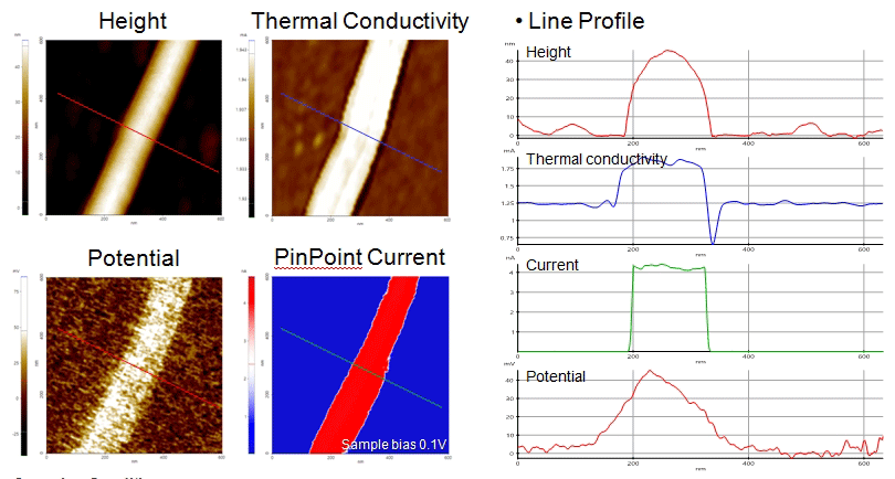
Scanning Conditions
- System: XE7
- Scan Mode: SThM, KPFM, PinPoint CP-AFM
- Cantilever: Nanothermal probe, NCST-Au (k=7.4N/m, f=160kHz), CDT-CONTR (k=0.5N/m, f=20kHz)
- Scan Size: 0.6μm×0.6μm
- Scan Rate: 0.5Hz, 0.5Hz, 0.15Hz
- Pixel: 256×128
- Scan Mode: SThM, KPFM, PinPoint CP-AFM
- Cantilever: Nanothermal probe, NCST-Au (k=7.4N/m, f=160kHz), CDT-CONTR (k=0.5N/m, f=20kHz)
- Scan Size: 0.6μm×0.6μm
- Scan Rate: 0.5Hz, 0.5Hz, 0.15Hz
- Pixel: 256×128