-
Modulus Lift Scanning_Thermal_Microscopy YszSubstrate PolymerBlend LiNbO3 ConductingPolymer Magnets ito_film Ucl IVSpectroscopy margarine Biology thermoplastic_elastomers HighResolution Bacteria 2-vinylpyridine FM-KPFM dichalcogenide Polarization tip_bias_mode Molybdenum Fujian Stiffness TungstenDeposition IIT-chennai Sulfur H-BN Copper MLCC Fluoride ScanningTunnelingMicroscopy Deposition GaP Logo
Report image
If you found this image unacceptable, please let us know. We will review your report and take action if we determine this image is really unacceptable.
Atomic steps on GaP(Gallium Phosphide) layer on Si
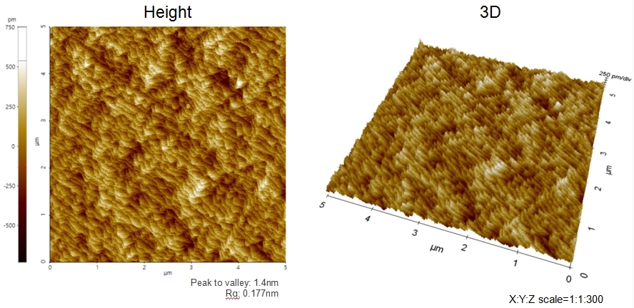
Scanning Conditions
- System: NX20
- Scan Mode: Non-contact
- Cantilever: PPP-NCHR (k=42N/m, f=300kHz)
- Scan Size: 5μm×5μm
- Scan Rate: 1Hz
- Pixel: 512×512