-
Molybdenum_disulfide mono_layer Ceramic Implant Lift Change INSP PolyStylene Oxide BoronNitride MultiferroicMaterials heterojunctions cannabis Fe_film medical thermal_property ContactModeDot Austenite temp Chemical Vapor Deposition Wonseok FFM multi_layer SicMosfet fluorocarbon Bmp PANI Tapping StainlessSteel India single_layer C60H122 CaMnO3 SingleLayer margarine
Report image
If you found this image unacceptable, please let us know. We will review your report and take action if we determine this image is really unacceptable.
LiNbO3 wafer
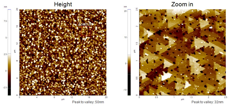
Scanning Conditions
- System: NX10
- Scan Mode: Non-contact
- Cantilever: AC55TS (k=85N/m, f=1600kHz)
- Scan Size:20μm×20μm, 2.5μm×2.5μm
- Scan Rate: 5Hz, 10Hz
- Pixel: 512×512, 256×256
- Scan Mode: Non-contact
- Cantilever: AC55TS (k=85N/m, f=1600kHz)
- Scan Size:20μm×20μm, 2.5μm×2.5μm
- Scan Rate: 5Hz, 10Hz
- Pixel: 512×512, 256×256