-
GalliumPhosphide AnodizedAluminumOxide MolybdenumDisulfide multi_layer HafniumDioxide Polyurethane SoftSample LaAlO3 Mechanical&nanotechnology P3HT LightEmission NUS LowDensityPolyethylene NCM ForceVolume ScratchMode NTU Mosfet PolymerPatterns Array GlassTemperature Aggregated_molecules gallium_nitride hard_disk_media small_scan CeramicCapacitor Co/Cr/Pt STM StrontiumTitanate Steps FAPbI3 HighAspect Writing Melt Pinpoint
Report image
If you found this image unacceptable, please let us know. We will review your report and take action if we determine this image is really unacceptable.
Copper film
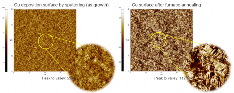
Scanning Conditions
- System : NX-Wafer
- Scan Mode: Non-contact
- Scan Rate : All 1Hz
- Scan Size : All 512μm×256μm
- Pixel Size : 512×512
- Cantilever : OMCL-AC160TS (k=26N/m, f=300kHz)