-
Switching WWafer Reduction HACrystal Electical&Electronics PtfeMembrane Pattern ScanningKelvinProbeMicroscopy HexagonalBN temperature controller AFM TriGlycineSulphate graphene_hybrid Tungsten_disulfide Sapphire Trench TappingMode BiVO4 NCM\ Resistance TransitionMetal self_assembly pinpoint mode molecular_beam MeltingPoint HexacontaneFilm LDPE thermal_property Formamidinium_lead_iodide Vortex Tapping Au111 tip_bias_mode MultiLayerCeramicCapacitor LifeScience Nanostructure
Report image
If you found this image unacceptable, please let us know. We will review your report and take action if we determine this image is really unacceptable.
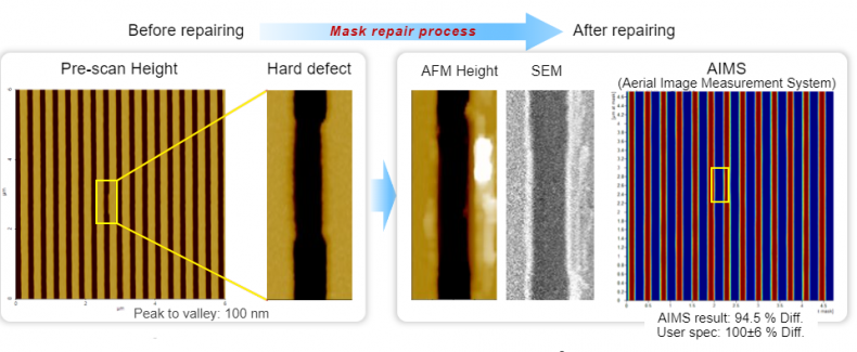
MoSi₂ Hard defect repair
Scanning Conditions
- System : NX-Mask
- Scan Mode: Non-contact for imaging Sweep for repairing
- Scan Rate : 0.3 Hz
- Scan Size : 6μm, 0.5μm×1μm
- Pixel Size : 512×64 for 6μm2, 512×34 for 0.5μm×1μm