-
Nanostructure AEAPDES PUR Ito BlockCopolymer RedBloodCell Conductive AFM tip_bias_mode LiftMode Electrical&Electronics AIN CHRYSALIS_INC Techcomp SetpointMode AtomicLayer LogAmplifier 3-hexylthiophene sputter ScanningTunnelingMicroscopy Collagen SSRM FAFailureAnlaysis Adhesive ReflexLens BaTiO3 Chemical Vapor Deposition Sio2 MechanicalProperties Lift LiquidCrystal ConductiveAFM LiftHeight medical Grain Metal
Report image
If you found this image unacceptable, please let us know. We will review your report and take action if we determine this image is really unacceptable.
PS/LPDE
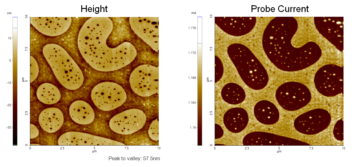
Spincast layer of PS/LDPE blend on Si. Signal change by thermal conductivity difference.
Scanning Conditions
- System: NX10
- Scan Mode: SThM
- Cantilever: NanoThermal Probe
- Scan Size: 10μm×10μm
- Scan Rate: 0.5Hz
- Pixel Size: 256 × 512
- Scan Mode: SThM
- Cantilever: NanoThermal Probe
- Scan Size: 10μm×10μm
- Scan Rate: 0.5Hz
- Pixel Size: 256 × 512