-
Pzt nanomechanical LaAlO3 LightEmission Organic PS_LDPE DataStorage cooling Croatia LMF Ferroelectric Phthalocyanine TyphimuriumBiofilm fifber Chemical Vapor Deposition BreastCancerCell polyvinyl acetate BiVO4 Ni-FeAlloy TungstenThinFilmDeposition SurfaceOxidation Carbon medical Growth #Materials 3-hexylthiophene ReflexLens PFM Tungsten_disulfide Iron Trench CNT Ananth GaN Magnetostrictive
Report image
If you found this image unacceptable, please let us know. We will review your report and take action if we determine this image is really unacceptable.
Monolayer Graphene on PDMS Surface
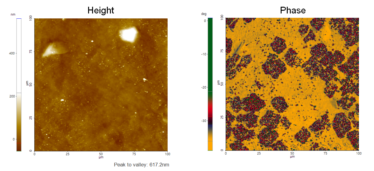
Monolayer Graphene grown on Cu foil using CVD process is transferred on to PDMS substrate.
Scanning Conditions
- System: NX20
- Scan Mode: Tapping
- Cantilever: Access-NC (k=113N/m, f=330kHz)
- Scan Size: 100μm×100μm
- Scan Rate: 0.6Hz
- Pixel Size: 256 × 256
- Scan Mode: Tapping
- Cantilever: Access-NC (k=113N/m, f=330kHz)
- Scan Size: 100μm×100μm
- Scan Rate: 0.6Hz
- Pixel Size: 256 × 256