-
SrO Liquid MoirePattern DLaTGS TungstenThinFilmDeposition Wang LiquidCell Aluminum Formamidinium_lead_iodide LightEmiting Steps exfoliate ItoGlass lithography Lateral_Force_Microscopy silicon_carbide FrictionalForceMicroscopy PtfeFilter KelvinProbeForceMicroscopy Platinum Sperm PrCurve HOPG Tin sulfide Metal TemperatureControlledAFM Switching ScanningIon-ConductanceMicroscopy INSPParis LMF FM_SKPM ThinFilm HighAspect AM_KPFM NUSNNI
Report image
If you found this image unacceptable, please let us know. We will review your report and take action if we determine this image is really unacceptable.
Trench Etch Profile on Si Wafer
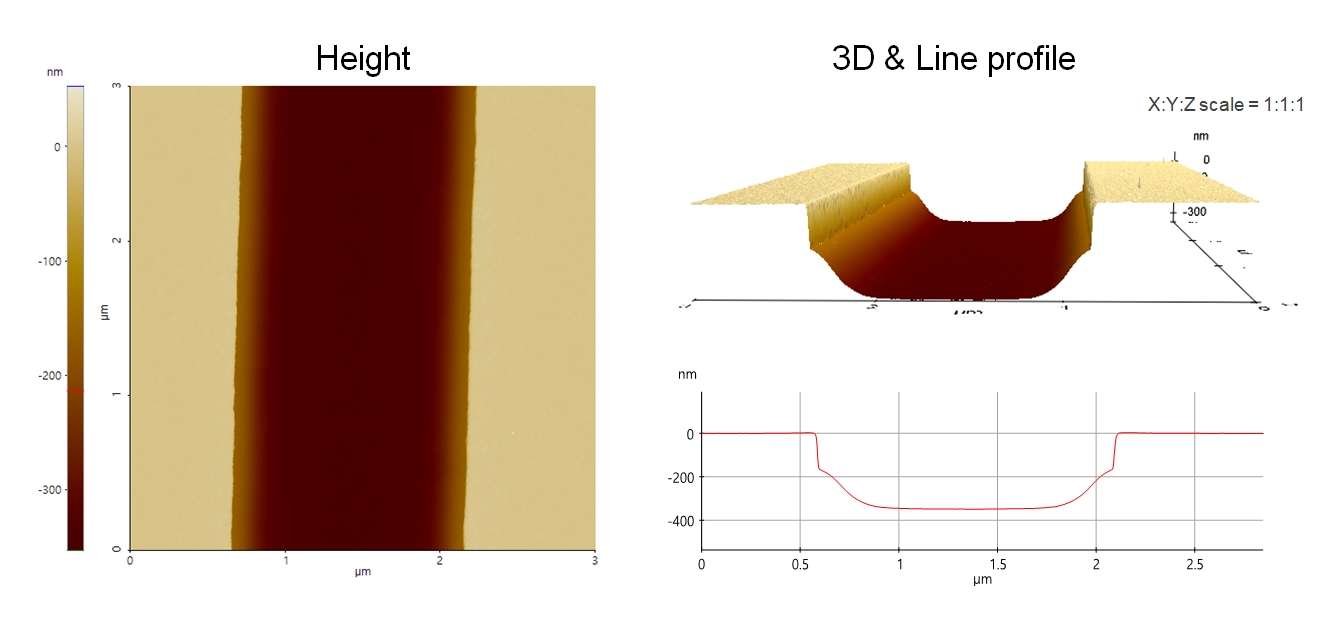
Top dielectric trench etch profile on Si wafer having tapered slope at the trench sidewall.
Scanning Conditions
- System: NX20
- Scan Mode: Non-contact
- Cantilever: AC160TS (k=26N/m, f=300kHz)
- Scan Size: 3μm×3μm
- Scan Rate: 0.21Hz
- Pixel: 1024 × 256
- Scan Mode: Non-contact
- Cantilever: AC160TS (k=26N/m, f=300kHz)
- Scan Size: 3μm×3μm
- Scan Rate: 0.21Hz
- Pixel: 1024 × 256