-
Domain Zagreb nanobar thermal_property Glass Fe_film kelvin probe force microscopy ContactMode OrganicCompound InorganicCompound Spincast Sic GlassTemp ChemicalCompound Wafer Ito Celebration hetero_structure MechanicalProperty HardDisk YszSubstrate OpticalWaveguide blended polymers Workfunction LithiumNiobate mfm_amplitude Sperm doped Platinum HydroGel CuParticle Materials AdhesionEnergy Magnetic Insulator
Report image
If you found this image unacceptable, please let us know. We will review your report and take action if we determine this image is really unacceptable.
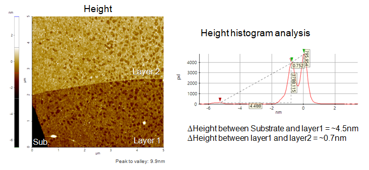
MoS2 Layers on SiO2
Scanning Conditions
- System: NX10
- Scan Mode: Non-contact
- Cantilever: AC160TS (k=26N/m, f=300kHz)
- Scan Size: 5μm×5μm
- Scan Rate: 1Hz
- Pixel Size: 256 × 256
- Scan Mode: Non-contact
- Cantilever: AC160TS (k=26N/m, f=300kHz)
- Scan Size: 5μm×5μm
- Scan Rate: 1Hz
- Pixel Size: 256 × 256