-
Heating molecular_beam Aggregated_molecules Metal ImideMonomer Pyroelectric domain_switching PECurve TemperatureControllerAFM PFM SSRM IIT-chennai LiquidCrystal Copolymer Ni-FeAlloy PolymerPatterns MBE CrystalGrowing Sulfur PolymerBlend NanoLithography PVA Organic molecular_self_assembly HDD LithiumNiobate Ram BlockCopolymer AM-KPFM MetalCompound StainlessSteel Fet Chrome block_copolymer Cobalt
Report image
If you found this image unacceptable, please let us know. We will review your report and take action if we determine this image is really unacceptable.
Atomic steps on GaP(Gallium Phosphide) layer on Si
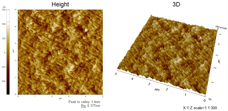
Scanning Conditions
- System: NX20
- Scan Mode: Non-contact
- Cantilever: PPP-NCHR (k=42N/m, f=300kHz)
- Scan Size: 5μm×5μm
- Scan Rate: 1Hz
- Pixel: 512×512