-
ThermalConductivity Photovoltaics Butterfly Singapore LiIonBattery Electronics PolycrystallineFerroelectricBCZT Molybdenum_disulfide SingleLayer Chemical Vapor Deposition margarine ReflexLens Etch single_layer Polarization Step Sphere EPFL SICM Writing MfmPhase TCS electrospinning AtomicLayer KelvinProbeForceMicroscopy Varistor Bismuth Piezoelectric TriGlycineSulphate Adhesion MolybdenumDisulfide WWafer self_healing TungstenDeposition SKKU
Report image
If you found this image unacceptable, please let us know. We will review your report and take action if we determine this image is really unacceptable.
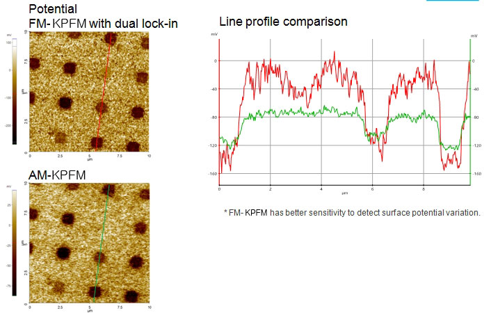
Polymer patterns on Si (2/2)

Scanning Conditions
- System: NX10
- Scan Mode: KPFM
- Cantilever: NSC36Cr-Au (k=1N/m, f=90kHz)
- Scan Size: 10μm×10μm
- Scan Rate: 0.2Hz
- Pixel: 512×256
