-
Hair DeflectionOptics FailureAnalysis Calcite PinpointNanomechanicalMode ImideMonomer single_layer HexacontaneFilm SrO Gong Cobalt Lanthanum_aluminate Force-distance Fujian Tin sulfide Bio SAM Biology Vacuum solar_cell ThermalConductivity mfm_amplitude KevlarFiber mono_layer Logo DIWafer ContactModeDots nanomechanical molecule BloodCell CP-AFM Conductance BariumTitanate Water TemperatureControl
Report image
If you found this image unacceptable, please let us know. We will review your report and take action if we determine this image is really unacceptable.
Tungsten coated wafer
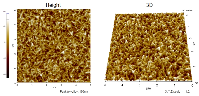
Scanning Conditions
- System: NX10
- Scan Mode: NCM
- Cantilever: NCHR (k=42N/m, f=300kHz)
- Scan Size: 5μm×5μm
- Scan Rate: 0.3Hz
- Pixel: 512×5126