-
PatternedSapphireSubstrat FM_KPFM Perovskite TemperatureControllerStage CastIron Cobalt-dopedIronOxide 2d_materials MetalCompound thermal_conductivity Boundary Grain PhaseChange Collagen Ferroelectric Optoelectonics Force-distance Global_Comm lift_mode ScanningSpreadingResistanceMicroscopy KevlarFiber TriGlycineSulphate Spain LiftHeight Polyvinylidene_fluoride Alloy Defect EFM SurfaceOxidation kelvin probe force microscopy medical temp_control Alkane FFM Conductance HardDiskMedia
Report image
If you found this image unacceptable, please let us know. We will review your report and take action if we determine this image is really unacceptable.
MoS2 (2/2)
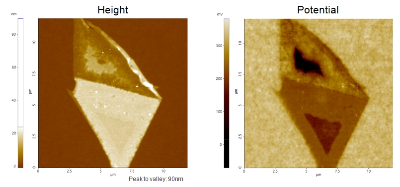
Scanning Conditions
- System: NX10
- Scan Mode: KPFM
- Cantilever: NSC36Cr-Au(k=1N/m, f=90kHz)
- Scan Size: 30μm×30μm,10μm×10μm
- Scan Rate: 0.1Hz
- Pixel: 512×1024