-
MechanicalProperties Adhesion MembraneFilter SrO Phenanthrene TemperatureControllerAFM MfmPhase Current ShenYang PyroelectricDetector Dental NusEce Ananth OrganicSemiconductor Hair PANI IcelandSpar SurfaceChange fifber Mechanical&nanotechnology FM_KPFM CaMnO3 MBE CrossSection OpticalWaveguide Ca10(PO4)6(OH)2 amplitude_modulation Liquid H-BN thermal_conductivity Filter Bismuth Spain Pinpoint IVSpectroscopy
Report image
If you found this image unacceptable, please let us know. We will review your report and take action if we determine this image is really unacceptable.
ITO Film Sputter Deposited onto Silicon
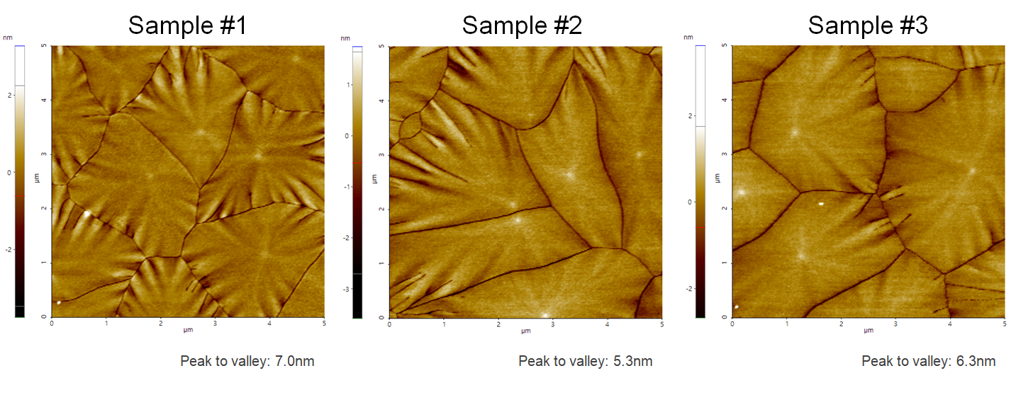
ITO-film, which was sputter deposited onto silicon. The grain size of those samples was influenced by changing the process settings in the Cluterline RAD sputter deposition system, one of the deposition tool platforms manufactured by Evatec.
Scanning Conditions
- System: NX10
- Scan Mode: Non-contact
- Cantilever: PPP-EFM (k=2.8N/m, f=75kHz)
- Scan Size: 5μm×5μm
- Scan Rate: 0.1Hz
- Pixel Size: 256 × 256
- Scan Mode: Non-contact
- Cantilever: PPP-EFM (k=2.8N/m, f=75kHz)
- Scan Size: 5μm×5μm
- Scan Rate: 0.1Hz
- Pixel Size: 256 × 256