-
ScratchMode Styrene membrane blended polymers Growing Biology Layer CHRYSALIS_INC Korea CompactDisk StrontiuTitanate Worcester_Polytechnic_Institute PtfeMembrane cannabinoid C_AFM Thermal Solution I-VSpectroscopy vertical_PFM hard_disk_media Pinpoint PFM pulsed_laser_deposition Vac ImideMonomer TemperatureControlledAFM LiquidCell AtomicLayer 2dMaterials Cell BiasMode mechanical_property ContactModeDots Array Graphene Morphology
Report image
If you found this image unacceptable, please let us know. We will review your report and take action if we determine this image is really unacceptable.
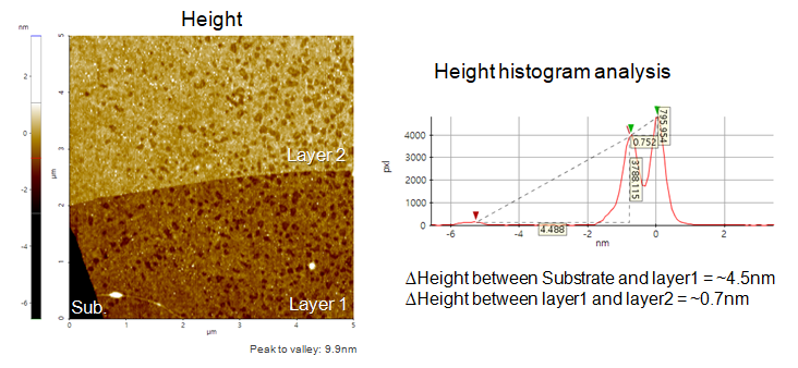
MoS2 Layers on SiO2
Scanning Conditions
- System: NX10
- Scan Mode: Non-contact
- Cantilever: AC160TS (k=26N/m, f=300kHz)
- Scan Size: 5μm×5μm
- Scan Rate: 1Hz
- Pixel Size: 256 × 256
- Scan Mode: Non-contact
- Cantilever: AC160TS (k=26N/m, f=300kHz)
- Scan Size: 5μm×5μm
- Scan Rate: 1Hz
- Pixel Size: 256 × 256