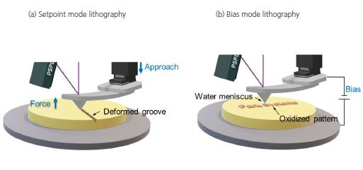
Atomic force microscopy (AFM) is recognized as a powerful tool for non-invasive imaging of sample surface topography. Especially, AFM is widely utilized to characterize various mechanical, physical, and chemical properties of materials at the nanoscale. Nonetheless, AFM can also be used to manipulate samples. Here, the AFM probe becomes a tool to modify the sample surface at nanometer resolution. This technique is known as Nanolithography. Compared to conventional lithography techniques such as focused ion beam lithography and electron beam lithography, the advantages of AFM-based Nanolithography lie in operational simplicity and cost-effectiveness. In Nanolithography, the sample surface can be modified based on three major modes: setpoint mode (force-assisted lithography), bias mode (bias-assisted lithography), and Z scanner mode (constant height lithography). In the setpoint mode, the tip applies a relatively large force to mechanically deform the sample surface by scratching it, as shown in figure 1 (a). Accordingly, the interaction between tip and sample is predominantly mechanical. In contrast, the bias mode uses a tip bias voltage to generate a pattern on the surface ofmetals or semiconductors. The combination of applied bias by the tip and water meniscus on the sample surface in an ambient environment can cause a redox reaction, leading to oxidation at the contact region, as shown in figure 1 (b). Lastly, lithography patterns can be attained by controlling the Z scanner position during measurement in Z scanner mode.
Figure 1. Schematic illustrations of (a) setpoint mode, and (b) bias mode lithography.
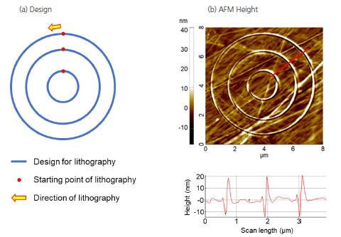
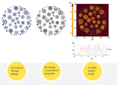
In Park Systems’ AFM, Nanolithography is provided in two ways: as the stand-alone SmartLitho software and as lithography mode embedded into the SmartScan software. Park Systems’ Nanolithography provides an independent and convenient drawing editor with a user-friendly interface, enabling users to easily design lithography patterns (e.g. point, line, circle, rectangle, and polygon) without further requirements from additional graphic design software. In addition, a pre-designed pattern (bitmap) can be also imported and mapped on the sample surface. Figure 2 (b) shows three different sizes of circle patterns generated by line drawing on a polycarbonate surface using the setpoint mode. For that, the AFM tip creates the scratches on the surface following the lithography direction in vector scan as shown in figure 2 (a). The scratch depth and width are dependent on the cantilever force constant value, setpoint, tip radius, and drawing speed. An example of bias mode lithography based on a pre-designed pattern (bitmap) is presented in figure 3. The tip bias was applied on the patterned area to create an oxidation layer on a bare silicon surface. The redox reaction requires a water meniscus at the AFM tip which naturally occurs in ambient conditions. The general thickness of the oxidation layer created by lithography is about 1 to 2 nm in height and is dependent on tip bias voltage, humidity, tip radius, and drawing speed. When a bitmap design is imported to SmartLitho software, the color of the design is converted to grayscale and the tip scans the surface in raster scan mode while applying different tip bias according to the gray level as shown in figure 3. In figure 3 (b), -10 V tip bias was applied at the darkest area of lithography design and no tip bias was applied at the white area.
Figure 2. Example of setpoint mode lithography measurement on a polycarbonate surface. The cantilever used is a diamond-coated cantilever tip with a force constant of 80 N/m. The scan rate was set to 0.5 Hz. For force-assisted lithography, a high force constant cantilever is useful in attaining sufficient contact pressure to permanently deform the sample and generate a lithography pattern.
Figure 3. Example of bias mode lithography obtained on a bare silicon substrate. The tip bias applied to the darkest area was -10 V. Scan rate were set to 0.5 Hz.
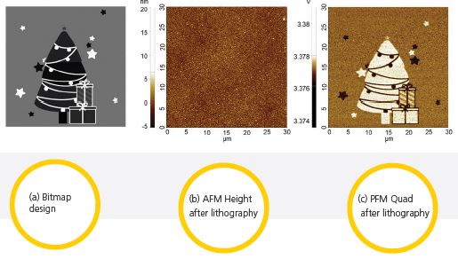
Figure 4. Domain switching on PZT thin film using tip bias mode. The images were obtained using piezoelectric force microscopy (PFM) mode after performing lithography with different applied tip biases. The tip bias applied to the black area of design was +10 V and the white area was -10 V for lithography.
Nanolithography can also be applied to study domain switching of ferroelectric materials. Figure 4 presents a pattern obtained on PZT thin film based on bias mode lithography. The surface shows no height difference after lithography, however, the ferroelectric domain of PZT can be switched by applying a tip bias, as shown in figure 4. In conventional Nanolithography, the available applied bias voltage ranges from -10 V to +10 V. For applications that need a higher voltage range, we have developed the high voltage Nanolithography mode that allows applying a DC bias up to ± 175 V. Thus, Park Systems’ Nanolithography offers a versatile and customizable tool kit to develop nanostructures and nanosystems such as nano transistors, nanologic gates, NEMS, and drug synthesis and delivery systems.


